Begeleide axonen; op weg naar meer inzicht in de werking van hersencellen
Wat hebben Kurt Cobain, Ronald Reagan, Vincent Van Gogh en Muhammad Ali gemeen? Naast hun bekendheid lijden ze ook aan een hersenaandoening, respectievelijk een bipolaire stoornis, alzheimer, depressie en parkinson. Ook in uw omgeving kent u wellicht mensen met dergelijke aandoeningen.
Het grote probleem
Het veelvuldig voorkomen van deze aandoeningen en de hoge kosten die hiermee gepaard gaan, 680 miljard euro in Europa alleen al, stimuleren het onderzoek naar de werking van de hersenen. Dankzij de ontwikkeling van nieuwe technologische technieken kunnen we ons inzicht en onze kennis vergroten.
Onze hersenen zijn opgebouwd uit een gigantisch aantal cellen. Ruw geschat heeft ieder van ons zo’n 86 miljard hersencellen of neuronen. Deze neuronen zijn opgebouwd uit 3 delen: een cellichaam, een netwerk van vertakte uitlopers ook wel dendrieten genoemd en tenslotte een lange uitloper die zorgt voor het doorgeven van prikkels, het axon. Hersencellen zenden continu elektrische signalen of pulsen naar elkaar. De plek waar een signaal van het ene neuron naar het andere springt, wordt de synaps genoemd
De oplossing
Om meer inzicht te krijgen in neurologische aandoeningen moeten we deze elektrische signalen beter kunnen meten. Verschillende technieken zijn hiervoor in ontwikkeling. Zo kan men deze pulsen “in vivo” meten; d.w.z. rechtstreeks in de hersenen met behulp van elektrodes. Deze methode is niet eenvoudig en vrij gevaarlijk. Het kan mogelijk hersenschade veroorzaken. Een alternatieve methode om meer te weten te komen over de processen die zich afspelen in de hersenen is het “in vitro” laten groeien van hersencellen. Hierbij worden cellen uit de hersenen verwijderd en in een laboratorium gekweekt op bvb. een chip met elektroden. Deze elektroden zijn beschikbaar in verschillende vormen, materialen en groottes en kunnen elektrische signalen opvangen.
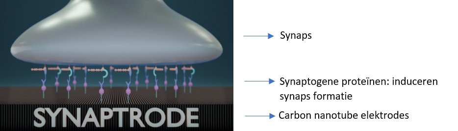
In het Haesler lab van NERF (Neuro-Electronics Research Flanders) wordt zo een nieuwe innovatieve ‘in vitro‘ elektrodetechnologie ontwikkeld waarbij neuronen synapsen vormen met elektrodes: de synaptrode interface. (zie afbeelding…)
De thesis
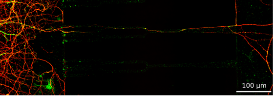
De elektrische signalen die we kunnen meten aan deze “synaptrodes” zijn ontzettend klein. Verstoringen of ruis moeten we dan ook zoveel mogelijk proberen te beperken. Zo zorgt de activiteit van cellichamen die in de nabijheid liggen van de neuronen voor ruis. Dit type ruis kunnen we vermijden door de synapsen te scheiden van de cellichamen. In mijn thesis werden 2 technieken onderzocht om deze scheiding te bewerkstelligen: kleine kanaaltjes gemaakt van een flexibel kunststofmateriaal en groeven direct uitgegraven in een chip. De axonen van de hersencellen kunnen zowel doorheen deze kanaaltjes als in de groeven uitgroeien. Zo komt een scheiding van cellichamen en synapsen tot stand en kan ruis in de elektrische signalen aan de synapsen voorkomen worden.

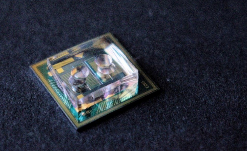
Voor de vervaardiging van de kanaaltjes gebruiken we een “molding” techniek. Deze techniek is vergelijkbaar met het maken van een gipsen afgietsel, maar dan op microschaal. We starten vanuit een “master” waar we een flexibel kunststofmateriaal op laten uitharden. Na uitharding van de kunststof en verwijdering van de master bekomen we kanaaltjes met slechts een dikte van 1/10e van een mensenhaar. Deze kanaaltjes brengen we daarna aan op een chip. Aan het ene uiteinde van de kanaaltjes plaatsen we de neuronen met hun cellichaam. De axonen van de neuronen kunnen dan door de kunststofkanaaltjes groeien om aan het andere uiteinde mogelijke synapsen te vormen.

Om groeven te maken, nemen we rechtstreeks materiaal weg van een chip. Ook deze groeven hebben een dikte van slechts 1/10e van een haar. De groeven begeleiden de axonen in hun groei.
Voor de uiteindelijke experimenten gebruikten we tijdens onze thesis hersencellen van muizen. Deze cellen werden aan het ene uiteinde van de structuur geplaatst en hadden dan 10 dagen de tijd om doorheen de kanaaltjes naar het andere uiteinde te groeien (Zie afbeelding). Na diverse tegenslagen zoals het afsterven van de hersencellen, uitdrogen van de kanaaltjes, contaminatie door bacteriën en schimmels, enz. lukte het om de neuronen doorheen de kanaaltjes te laten groeien. Voor het vervolg van het onderzoek, het vormen van synapsen na groei door de kanaaltjes, zijn bijkomende experimenten nodig.
Als gevolg van de Covid-19-omstandigheden kon geen onderzoek opgestart worden naar de werking van de groeven.
De toekomst
De weg naar behandeling van neurologische aandoeningen is nog lang. Wetenschappelijk onderzoek en nieuwe technologische technieken moeten zorgen voor voortschrijdend inzicht. Het onderwerp van deze thesis, nl. het ontwikkelen van technieken om de kwaliteit van het meten van de elektrische activiteit aan de synapsen van de hersencellen te verhogen, vormt een bescheiden stap in een “never ending (re)search story”.
Bibliografie
[1] B. J. Larson, “A Review of the History of Electrophysiology and Electroencephalography.
Part II,” American Journal of EEG Technology, vol. 3, pp. 61–64, sep 1963.
[2] J. Bernsten, Untersuchungen über den erregungsvirgang im Nerven- und Muskelsysteme.
Heidelberg: Carl Winters Universitätsbuchhandelung, 1871.
[3] L. Galvani, De viribus electricitatis in motu musculari commentarius. 1791.
[4] K. Czöndör, M. Garcia, A. Argento, A. Constals, C. Breillat, B. Tessier, and
O. Thoumine, “Micropatterned substrates coated with neuronal adhesion molecules
for high-content study of synapse formation,” Nature Communications, vol. 4, p. 2252,
aug 2013.
[5] K. Lepeta, M. V. Lourenco, B. C. Schweitzer, P. V. Martino Adami, P. Banerjee,
S. Catuara-Solarz, M. de La Fuente Revenga, A. M. Guillem, M. Haidar, O. M. Ijomone,
B. Nadorp, L. Qi, N. D. Perera, L. K. Refsgaard, K. M. Reid, M. Sabbar, A. Sahoo,
N. Schaefer, R. K. Sheean, A. Suska, R. Verma, C. Vicidomini, D. Wright, X.-D. Zhang,
and C. Seidenbecher, “Synaptopathies: synaptic dysfunction in neurological disorders -
A review from students to students,” Journal of neurochemistry, vol. 138, pp. 785–805,
sep 2016.
[6] A. M. Belle, H. A. Enright, A. P. Sales, K. Kulp, J. Osburn, E. A. Kuhn, N. O. Fischer,
and E. K. Wheeler, “Evaluation of in vitro neuronal platforms as surrogates for in vivo
whole brain systems,” Scientific reports, vol. 8, p. 10820, jul 2018.
[7] M. K. B. Jonsson, T. A. B. van Veen, J. Synnergren, and B. Becker, “Towards Creating
the Perfect In Vitro Cell Model,” Stem cells international, vol. 2016, p. 3459730, 2016.
[8] L. Conforti, “Patch-Clamp Techniques,” in Methods in Cell Biology (N. B. T. C. P. S.
B. F. E. Sperelakis, ed.), ch. Chapter 20, pp. 369–381, San Diego: Academic Press,
2012.
[9] M. E. J. Obien, K. Deligkaris, T. Bullmann, D. J. Bakkum, and U. Frey, “Revealing
neuronal function through microelectrode array recordings,” Frontiers in Neuroscience,
vol. 8, p. 423, 2015.
[10] P. Shi, M. A. Scott, B. Ghosh, D.Wan, Z. Wissner-Gross, R. Mazitschek, S. J. Haggarty,
and M. F. Yanik, “Synapse microarray identification of small molecules that enhance
synaptogenesis,” Nature Communications, vol. 2, no. 1, p. 510, 2011.
[11] C. Hammond, “Chapter 1 - Neurons,” in Cellular and Molecular Neurophysiology
(Fourth edition) (C. B. T. C. Hammond and M. N. F. Edition), eds.), ch. 1, pp. 3–23,
Boston: Academic Press, 2015.
[12] G. Stuart, N. Sprutson, and M. Häusser, Dendrites. New York: Oxford University
Press, 3 ed., 2016.
[13] C. Hammond and M. Esclapez, “Chapter 6 - The chemical synapses,” in Cellular
and Molecular Neurophysiology (Fourth edition) (C. B. T. C. Hammond and M. N. F.
Edition), eds.), ch. 6, pp. 121–144, Boston: Academic Press, 2015.
[14] C. Hammond, O. El Far, and M. Seagar, “Chapter 7 - Neurotransmitter release,” in
Cellular and Molecular Neurophysiology (Fourth edition) (C. B. T. C. Hammond and
M. N. F. Edition), eds.), ch. 7, pp. 145–169, Boston: Academic Press, 2015.
[15] J. L. Goldberg, “How does an axon grow ?,” Genes & Dev., vol. 17, no. 650, pp. 941–958,
2003.
[16] H. Lodish, A. Berk, and S. Zipursky, “The Action Potential and Conduction of Electric
Impulses,” in Molecular Cell Biology, ch. Section 21, W. H. Freeman, 2000.
[17] M. D. Forrest, “The sodium-potassium pump is an information processing element in
brain computation,” Frontiers in Physiology, vol. 5, p. 472, 2014.
[18] G. J. Kress and S. Mennerick, “Action potential initiation and propagation: upstream
influences on neurotransmission,” Neuroscience, vol. 158, pp. 211–222, jan 2009.
[19] T. C. Südhof and R. C. Malenka, “Understanding synapses: past, present, and future,”
Neuron, vol. 60, pp. 469–476, nov 2008.
[20] P. Scheiffele, J. Fan, J. Choih, R. Fetter, and T. Serafini, “Neuroligin Expressed in
Nonneuronal Cells Triggers Presynaptic Development in Contacting Axons,” Cell,
vol. 101, pp. 657–669, jun 2000.
[21] J. Jeon, M.-A. Oh, W. Cho, S.-H. Yoon, J. Y. Kim, and T. D. Chung, “Robust Induced
Presynapse on Artificial Substrates as a Neural Interfacing Method,” ACS Applied
Materials & Interfaces, vol. 11, pp. 7764–7773, feb 2019.
[22] D. Schreiner, J. N. Savas, E. Herzog, N. Brose, and J. de Wit, “Synapse biology in the
circuit-age paths toward molecular connectomics,” Current Opinion in Neurobiology,
vol. 42, pp. 102–110, 2017.
[23] D. Bagnard, “Molecular mechanisms of axonal growth,” in Axon Growth and Guidance,
vol. 621, ch. Chapter 1:, pp. 1–12, Springer, jan 2007.
[24] L. A. Lowery and D. V. Vactor, “The trip of the tip: understanding the growth cone
machinery,” Nature Reviews Molecular Cell Biology, vol. 10, no. 5, pp. 332–343, 2009.
[25] H. M. Buettner, R. N. Pittman, and J. K. Ivins, “A Model of Neurite Extension across
Regions of Nonpermissive Substrate: Simulations Based on Experimental Measurement
of Growth Cone Motility and Filopodial Dynamics,” Developmental Biology, vol. 163,
no. 2, pp. 407–422, 1994.
[26] D. Šmít, C. Fouquet, F. Pincet, M. Zapotocky, and A. Trembleau, “Axon tension
regulates fasciculation/defasciculation through the control of axon shaft zippering,”
eLife, vol. 6, p. e19907, apr 2017.
[27] A. S. f. N. George J. Siegel, R. Wayne Albers, Scott Brady, Donald L. Price, “Basic
neurochemistry: Molecular, cellular and medical aspects, ed 5. Edited by George, J.
Siegel, Bernard W. Agranoff, R. Wayne Albers, and Perry B. Molinoff New York,
Raven Press, 1994, 1080 pp, illustrated, $84.00,” Annals of Neurology, vol. 36, p. 121,
jul 1994.
[28] M. Tessier-Lavigne and C. Goodman, “The Molecular Biology of Axon Guidance,”
Science (New York, N.Y.), vol. 274, pp. 1123–1133, dec 1996.
[29] J. Tang, U. Rutishauser, and L. Landmesser, “Polysialic acid regulates growth cone
behavior during sorting of motor axons in the plexus region,” Neuron, vol. 13, no. 2,
pp. 405–414, 1994.
[30] L. M. Y. Yu, N. D. Leipzig, and M. S. Shoichet, “Promoting neuron adhesion and
growth,” Materials Today, vol. 11, no. 5, pp. 36–43, 2008.
[31] M. Gonzalez, X. Guo, M. Lin, M. Stancescu, P. Molnar, S. Spradling, and J. J.
Hickman, “Polarity Induced in Human Stem Cell Derived Motoneurons on Patterned
Self-Assembled Monolayers,” ACS Chemical Neuroscience, vol. 10, pp. 2756–2764, jun
2019.
[32] O. Feinerman, A. Rotem, and E. Moses, “Reliable neuronal logic devices from patterned
hippocampal cultures,” Nature Physics, vol. 4, no. 12, pp. 967–973, 2008.
[33] S. K. W. Dertinger, X. Jiang, Z. Li, V. N. Murthy, and G. M. Whitesides, “Gradients
of substrate-bound laminin orient axonal specification of neurons,” Proceedings of the
National Academy of Sciences, vol. 99, pp. 12542 LP – 12547, oct 2002.
[34] S. Willerth, “Chapter 4 - Design considerations when engineering neural tissue from
stem cells,” in Engineering Neural Tissue from Stem Cells (S. B. T. E. N. T. f. S. C.
Willerth, ed.), ch. 4, pp. 65–88, Academic Press, 1 ed., 2017.
[35] T. B. DeMarse, L. Pan, S. Alagapan, G. J. Brewer, and B. C. Wheeler, “Feed-Forward
Propagation of Temporal and Rate Information between Cortical Populations during
Coherent Activation in Engineered In Vitro Networks,” Frontiers in neural circuits,
vol. 10, p. 32, apr 2016.
[36] L. Pan, S. Alagapan, E. Franca, S. S. Leondopulos, T. B. DeMarse, G. J. Brewer,
and B. C. Wheeler, “An in vitro method to manipulate the direction and functional
strength between neural populations,” Frontiers in neural circuits, vol. 9, p. 32, jul
2015.
[37] Y. Takayama, N. Kotake, T. Haga, T. Suzuki, and K. Mabuchi, “Formation of oneway-
structured cultured neuronal networks in microfluidic devices combining with
micropatterning techniques,” Journal of Bioscience and Bioengineering, vol. 114, no. 1,
pp. 92–95, 2012.
[38] M. K. Lewandowska, D. J. Bakkum, S. B. Rompani, and A. Hierlemann, “Recording
Large Extracellular Spikes in Microchannels along Many Axonal Sites from Individual
Neurons,” PLOS ONE, vol. 10, p. e0118514, mar 2015.
[39] R. van de Wijdeven, O. H. Ramstad, V. D. Valderhaug, P. Köllensperger, A. Sandvig,
I. Sandvig, and Ø. Halaas, “A novel lab-on-chip platform enabling axotomy and
neuromodulation in a multi-nodal network,” Biosensors and Bioelectronics, vol. 140,
p. 111329, 2019.
[40] E. Malishev, A. Pimashkin, A. Gladkov, Y. Pigareva, A. Bukatin, V. Kazantsev,
I. Mukhina, and M. Dubina, “Microfluidic device for unidirectional axon growth,”
Journal of Physics: Conference Series, vol. 643, p. 12025, 2015.
[41] J.-M. Peyrin, B. Deleglise, L. Saias, M. Vignes, P. Gougis, S. Magnifico, S. Betuing,
M. Pietri, J. Caboche, P. Vanhoutte, J.-L. Viovy, and B. Brugg, “Axon diodes for the
reconstruction of oriented neuronal networks in microfluidic chambers,” Lab on a Chip,
vol. 11, no. 21, pp. 3663–3673, 2011.
[42] B. J. Dworak and B. C. Wheeler, “Novel MEA platform with PDMS microtunnels
enables the detection of action potential propagation from isolated axons in culture,”
Lab on a Chip, vol. 9, no. 3, pp. 404–410, 2009.
[43] J. le Feber, W. Postma, E. de Weerd, M. Weusthof, and W. L. C. Rutten, “Barbed
channels enhance unidirectional connectivity between neuronal networks cultured on
multi electrode arrays,” Frontiers in neuroscience, vol. 9, p. 412, nov 2015.
[44] A. Gladkov, Y. Pigareva, D. Kutyina, V. Kolpakov, A. Bukatin, I. Mukhina, V. Kazantsev,
and A. Pimashkin, “Design of Cultured Neuron Networks in vitro with Predefined
Connectivity Using Asymmetric Microfluidic Channels,” Scientific Reports, vol. 7,
no. 1, p. 15625, 2017.
[45] J. Mai, L. Fok, H. Gao, X. Zhang, and M.-m. Poo, “Axon Initiation and Growth Cone
Turning on Bound Protein Gradients,” The Journal of Neuroscience, vol. 29, pp. 7450
LP – 7458, jun 2009.
[46] J. Cools, D. Copic, Z. Luo, G. Callewaert, D. Braeken, and M. De Volder, “3D
Microstructured Carbon Nanotube Electrodes for Trapping and Recording Electrogenic
Cells,” Advanced Functional Materials, vol. 27, p. 1701083, sep 2017.
[47] J. J. FitzGerald, S. P. Lacour, S. B. McMahon, and J. W. Fawcett, “Microchannels
as Axonal Amplifiers,” IEEE Transactions on Biomedical Engineering, vol. 55, no. 3,
pp. 1136–1146, 2008.
[48] L. Pan, S. Alagapan, E. Franca, T. DeMarse, G. J. Brewer, and B. C. Wheeler, “Large
extracellular spikes recordable from axons in microtunnels,” IEEE transactions on
neural systems and rehabilitation engineering : a publication of the IEEE Engineering
in Medicine and Biology Society, vol. 22, pp. 453–459, may 2014.
[49] R. M. Smeal, R. Rabbitt, R. Biran, and P. A. Tresco, “Substrate Curvature Influences
the Direction of Nerve Outgrowth,” Annals of Biomedical Engineering, vol. 33, no. 3,
pp. 376–382, 2005.
[50] J. S. Chua, C.-P. Chng, A. A. K. Moe, J. Y. Tann, E. L. K. Goh, K.-H. Chiam, and
E. K. F. Yim, “Extending neurites sense the depth of the underlying topography
during neuronal differentiation and contact guidance,” Biomaterials, vol. 35, no. 27,
pp. 7750–7761, 2014.
[51] B. Black, V. Vishwakarma, K. Dhakal, S. Bhattarai, P. Pradhan, A. Jain, Y.-t. Kim,
and S. Mohanty, “Spatial temperature gradients guide axonal outgrowth,” Scientific
Reports, vol. 6, p. 29876, jul 2016.
[52] D. E. Koser, A. J. Thompson, S. K. Foster, A. Dwivedy, E. K. Pillai, G. K. Sheridan,
H. Svoboda, M. Viana, L. d. F. Costa, J. Guck, C. E. Holt, and K. Franze,
“Mechanosensing is critical for axon growth in the developing brain,” Nature Neuroscience,
vol. 19, p. 1592, sep 2016.
[53] T. Honegger, M. A. Scott, M. F. Yanik, and J. Voldman, “Electrokinetic confinement
of axonal growth for dynamically configurable neural networks,” Lab on a Chip, vol. 13,
no. 4, pp. 589–598, 2013.
[54] D. J. Stevenson, T. K. Lake, B. Agate, V. Garcés-Chávez, K. Dholakia, and F. Gunn-
Moore, “Optically guided neuronal growth at near infrared wavelengths,” Opt. Express,
vol. 14, no. 21, pp. 9786–9793, 2006.
[55] L. Gu, B. Black, S. Ordonez, A. Mondal, A. Jain, and S. Mohanty, “Microfluidic
control of axonal guidance,” Scientific Reports, vol. 4, p. 6457, oct 2014.
[56] C. Miller, S. Jeftinija, and S. Mallapragada, “Synergistic Effects of Physical and
Chemical Guidance Cues on Neurite Alignment and Outgrowth on Biodegradable
Polymer Substrates,” Tissue Engineering, vol. 8, pp. 367–378, jul 2002.
[57] A. Rajnicek, S. Britland, and C. McCaig, “Contact guidance of CNS neurites on
grooved quartz: influence of groove dimensions, neuronal age and cell type,” Journal
of Cell Science, vol. 110, pp. 2905 LP – 2913, dec 1997.
[58] Y.-A. Huang, C. T. Ho, Y.-H. Lin, C.-J. Lee, S.-M. Ho, M.-C. Li, and E. Hwang,
“Nanoimprinted Anisotropic Topography Preferentially Guides Axons and Enhances
Nerve Regeneration,” Macromolecular Bioscience, vol. 18, p. 1800335, dec 2018.
[59] R. Barillé, R. Janik, S. Kucharski, J. Eyer, and F. Letournel, “Photo-responsive
polymer with erasable and reconfigurable micro- and nano-patterns: An in vitro study
for neuron guidance,” Colloids and Surfaces B: Biointerfaces, vol. 88, no. 1, pp. 63–71,
2011.
[60] B. Kaehr, R. Allen, D. J. Javier, J. Currie, and J. B. Shear, “Guiding neuronal
development with in situ microfabrication,” Proceedings of the National Academy of
Sciences of the United States of America, vol. 101, pp. 16104 LP – 16108, nov 2004.
[61] C. Simitzi, A. Ranella, and E. Stratakis, “Controlling the morphology and outgrowth
of nerve and neuroglial cells: The effect of surface topography,” Acta Biomaterialia,
vol. 51, pp. 21–52, 2017.
[62] J. W. Lee, K. S. Lee, N. Cho, B. K. Ju, K. B. Lee, and S. H. Lee, “Topographical
guidance of mouse neuronal cell on SiO2 microtracks,” Sensors and Actuators B:
Chemical, vol. 128, no. 1, pp. 252–257, 2007.
[63] J. Zhang, S. Venkataramani, H. Xu, Y.-K. Song, H.-K. Song, G. T. R. Palmore,
J. Fallon, and A. V. Nurmikko, “Combined topographical and chemical micropatterns
for templating neuronal networks,” Biomaterials, vol. 27, no. 33, pp. 5734–5739, 2006.
[64] M. J. Mahoney, R. R. Chen, J. Tan, and W. Mark Saltzman, “The influence of
microchannels on neurite growth and architecture,” Biomaterials, vol. 26, no. 7,
pp. 771–778, 2005.
[65] A. Béduer, C. Vieu, F. Arnauduc, J.-C. Sol, I. Loubinoux, and L. Vaysse, “Engineering
of adult human neural stem cells differentiation through surface micropatterning,”
Biomaterials, vol. 33, no. 2, pp. 504–514, 2012.
[66] W. Li, Q. Y. Tang, A. D. Jadhav, A. Narang, W. X. Qian, P. Shi, and S. W. Pang,
“Large-scale Topographical Screen for Investigation of Physical Neural-Guidance Cues,”
Scientific Reports, vol. 5, p. 8644, mar 2015.
[67] J. Terryn, M. Welkenhuysen, O. Krylychkina, A. Firrincieli, A. Andrei, V. Reumers,
P. Van Damme, D. Braeken, and C. Verfaillie, “Topographical Guidance of PSC-Derived
Cortical Neurons,” Journal of Nanomaterials, vol. 2018, pp. 1–10, oct 2018.
[68] B. L. Leigh, K. Truong, R. Bartholomew, M. Ramirez, M. R. Hansen, and C. A.
Guymon, “Tuning Surface and Topographical Features to Investigate Competitive
Guidance of Spiral Ganglion Neurons,” ACS Applied Materials & Interfaces, vol. 9,
pp. 31488–31496, sep 2017.
[69] D. Y. Fozdar, J. Y. Lee, C. E. Schmidt, and S. Chen, “Hippocampal neurons respond
uniquely to topographies of various sizes and shapes,” Biofabrication, vol. 2, no. 3,
p. 35005, 2010.
[70] N. Gomez, S. Chen, and C. E. Schmidt, “Polarization of hippocampal neurons with
competitive surface stimuli: contact guidance cues are preferred over chemical ligands,”
Journal of the Royal Society, Interface, vol. 4, pp. 223–233, apr 2007.
[71] N. Gomez, Y. Lu, S. Chen, and C. E. Schmidt, “Immobilized nerve growth factor
and microtopography have distinct effects on polarization versus axon elongation in
hippocampal cells in culture,” Biomaterials, vol. 28, no. 2, pp. 271–284, 2007.
[72] H. Francisco, B. B. Yellen, D. S. Halverson, G. Friedman, and G. Gallo, “Regulation of
axon guidance and extension by three-dimensional constraints,” Biomaterials, vol. 28,
no. 23, pp. 3398–3407, 2007.
[73] J. A. Fantuzzo, R. P. Hart, J. D. Zahn, and Z. P. Pang, “Compartmentalized Devices as
Tools for Investigation of Human Brain Network Dynamics,” Developmental Dynamics,
vol. 248, pp. 65–77, jan 2019.
[74] R. Habibey, S. Latifi, H. Mousavi, M. Pesce, E. Arab-Tehrany, and A. Blau, “A
multielectrode array microchannel platform reveals both transient and slow changes in
axonal conduction velocity,” Scientific Reports, vol. 7, no. 1, p. 8558, 2017.
[75] N. Hong, S. Joo, and Y. Nam, “Characterization of Axonal Spikes in Cultured Neuronal
Networks Using Microelectrode Arrays and Microchannel Devices,” IEEE Transactions
on Biomedical Engineering, vol. 64, no. 2, pp. 492–498, 2017.
[76] R. Renault, J.-B. Durand, J.-L. Viovy, and C. Villard, “Asymmetric axonal edge
guidance: a new paradigm for building oriented neuronal networks,” Lab on a Chip,
vol. 16, no. 12, pp. 2188–2191, 2016.
[77] R. Habibey, A. Golabchi, S. Latifi, F. Difato, and A. Blau, “A microchannel device
tailored to laser axotomy and long-term microelectrode array electrophysiology of
functional regeneration,” Lab on a Chip, vol. 15, no. 24, pp. 4578–4590, 2015.
[78] R. Habibey, A. Golabchi, and A. Blau, “Microchannel Scaffolds for Neural Signal
Acquisition and Analysis BT - Neurotechnology, Electronics, and Informatics,” (Cham),
pp. 47–64, Springer International Publishing, 2015.
[79] R. Renault, N. Sukenik, S. Descroix, L. Malaquin, J.-L. Viovy, J.-M. Peyrin, S. Bottani,
P. Monceau, E. Moses, and M. Vignes, “Combining Microfluidics, Optogenetics and
Calcium Imaging to Study Neuronal Communication In Vitro,” PLOS ONE, vol. 10,
p. e0120680, apr 2015.
[80] K. Shimba, K. Sakai, T. Isomura, K. Kotani, and Y. Jimbo, “Axonal conduction
slowing induced by spontaneous bursting activity in cortical neurons cultured in a
microtunnel device,” Integrative Biology, vol. 7, pp. 64–72, nov 2014.
[81] K. Shimba, A. Saito, A. Takeuchi, Y. Takayama, K. Kotani, and Y. Jimbo, “Neural
Transplantation Model Using Integration Co-Culture Chamber,” Electronics and
Communications in Japan, vol. 97, pp. 36–43, feb 2014.
[82] P. Wieringa, R. Wiertz, E. de Weerd, and W. Rutten, “Bifurcating microchannels as a
scaffold to induce separation of regenerating neurites,” Journal of neural engineering,
vol. 7, p. 16001, feb 2010.
[83] R. Morales, M. Riss, L. Wang, R. Gavín, J. A. Del Río, R. Alcubilla, and E. Claverol-
Tinturé, “Integrating multi-unit electrophysiology and plastic culture dishes for network
neuroscience,” Lab on a Chip, vol. 8, no. 11, pp. 1896–1905, 2008.
[84] E. Claverol-Tinture, J. Cabestany, and X. Rosell, “Multisite Recording of Extracellular
Potentials Produced by Microchannel-Confined Neurons In-Vitro,” IEEE Transactions
on Biomedical Engineering, vol. 54, no. 2, pp. 331–335, 2007.
[85] A. M. Taylor, M. Blurton-Jones, S. W. Rhee, D. H. Cribbs, C. W. Cotman, and
N. L. Jeon, “A microfluidic culture platform for CNS axonal injury, regeneration and
transport,” Nature Methods, vol. 2, no. 8, pp. 599–605, 2005.
[86] P. M. Holloway, G. I. Hallinan, M. Hegde, S. I. R. Lane, K. Deinhardt, and J. West,
“Asymmetric confinement for defining outgrowth directionality,” Lab on a Chip, vol. 19,
no. 8, pp. 1484–1489, 2019.
[87] T. Akashi and Y. Yoshimura, “Deep reactive ion etching of borosilicate glass using an
anodically bonded silicon wafer as an etching mask,” Journal of Micromechanics and
Microengineering, vol. 16, no. 5, pp. 1051–1056, 2006.
[88] F. Laermer, S. Franssila, L. Sainiemi, and K. Kolari, “Chapter 21 - Deep Reactive Ion
Etching,” in Micro and Nano Technologies (M. Tilli, T. Motooka, V.-M. Airaksinen,
S. Franssila, M. Paulasto-Kröckel, V. B. T. H. o. S. B. M. M. Lindroos, and T. S.
Edition), eds.), pp. 444–469, Boston: William Andrew Publishing, 2015.
[89] K. Nojiri, Dry Etching Technology for Semiconductors. Springer, jan 2015.
[90] H. Jansen, H. Gardeniers, and M. D. Boer, “A survey on the reactive ion etching of
silicon in microtechnology,” Journal of Micromechanics and Microengineering, vol. 6,
no. 1, 1996.
[91] S. Mobini, Y. H. Song, M. W. McCrary, and C. E. Schmidt, “Advances in ex vivo
models and lab-on-a-chip devices for neural tissue engineering,” Biomaterials, vol. 198,
pp. 146–166, 2019.
[92] S. Kim, J. Park, A. Han, and J. Li, “Microfluidic systems for axonal growth and
regeneration research,” Neural regeneration research, vol. 9, pp. 1703–1705, oct 2014.
[93] R. B. Campenot, “Local control of neurite development by nerve growth factor,”
Proceedings of the National Academy of Sciences of the United States of America,
vol. 74, pp. 4516–4519, oct 1977.
[94] B. Gale, A. Jafek, C. Lambert, B. Goenner, H. Moghimifam, U. Nze, and S. Kamarapu,
“A Review of Current Methods in Microfluidic Device Fabrication and Future
Commercialization Prospects,” Inventions, vol. 3, p. 60, aug 2018.
[95] Y. Xia and G. M. Whitesides, “SOFT LITHOGRAPHY,” Annual Review of Materials
Science, vol. 28, pp. 153–184, aug 1998.
[96] P. Kim, K. W. Kwon, M. Park, S. Lee, S. M. Kim, and K. Suh, “Soft Lithography for
Microfluidics: a Review,” Biochip Journal, vol. 2(1), mar 2008.
[97] A. M. Collins, “Chapter 5 - Physical Techniques,” in Nanotechnology Cookbook (A. M.
B. T. N. C. Collins, ed.), ch. chapter 5, pp. 205–253, Oxford: Elsevier, 2012.
[98] J. A. Rogers and R. G. Nuzzo, “Recent progress in soft lithography,” Materials Today,
vol. 8, no. 2, pp. 50–56, 2005.
[99] S. K. Sia and G. M. Whitesides, “Microfluidic devices fabricated in
Poly(dimethylsiloxane) for biological studies,” ELECTROPHORESIS, vol. 24, pp. 3563–
3576, nov 2003.
[100] V. C. Pinto, P. J. Sousa, V. F. Cardoso, and G. Minas, “Optimized SU-8 Processing for
Low-Cost Microstructures Fabrication without Cleanroom Facilities. Micromachines,”
Micromachines, vol. 5, no. 3, pp. 783–755, 2014.
[101] J. Friend and L. Yeo, “Fabrication of microfluidic devices using polydimethylsiloxane,”
Biomicrofluidics, vol. 4, p. 26502, mar 2010.
[102] A. Campo and C. Greiner, “SU-8: a photoresist for high-aspect-ratio and 3D submicron
lithography,” J. Micromech. Microeng, vol. 17, pp. 81–95, jun 2007.
[103] F. Ceyssens and R. Puers, “SU-8 Photoresist BT,” in Encyclopedia of Nanotechnology
(B. Bhushan, ed.), pp. 2530–2543, Dordrecht: Springer Netherlands, 2012.
[104] J.-B. Lee, K.-H. Choi, and K. Yoo, “Innovative SU-8 Lithography Techniques and
Their Applications,” Micromachines, vol. 6, pp. 1–18, jan 2015.
[105] N. C. LaBianca and J. D. Gelorme, “High-aspect-ratio resist for thick-film applications,”
Advanced Lithography, 1995.
[106] R. Martinez-Duarte and M. Madou, “SU-8 Photolithography and Its Impact on Microfluidics,”
in Microfluidics and Nanofluidics Handbook: Fabrication, Implementation,
and Applications, pp. 231–268, CRC Press, sep 2010.
[107] J. V. Crivello and J. H. W. Lam, “Photoinitiated cationic polymerization with triarylsulfonium
salts,” Journal of Polymer Science Part A: Polymer Chemistry, vol. 34,
no. 16, pp. 3231–3253, 1996.
[108] J. M. Shaw, J. D. Gelorme, N. C. LaBianca, W. E. Conley, and S. J. Holmes, “Negative
photoresists for optical lithography,” IBM Journal of Research and Development,
vol. 41, no. 1.2, pp. 81–94, 1997.
[109] E. Koukharenko, M. Kraft, G. Ensell, and N. Hollinshead, “A comparative study of
different thick photoresists for MEMS applications,” Journal of Materials Science:
Materials in Electronics, vol. 16, pp. 741–747, nov 2005.
[110] D. C. Duffy, J. C. McDonald, O. J. A. Schueller, and G. M. Whitesides, “Rapid
Prototyping of Microfluidic Systems in Poly(dimethylsiloxane),” Analytical Chemistry,
vol. 70, pp. 4974–4984, dec 1998.
[111] R. Boya and G. Kulkarni, “Micromolding. A Soft Lithography Technique,” in Micromanufacturing
Processes, pp. 329–347, Taylor & Francis, oct 2012.
[112] T. Fujii, “PDMS-based microfluidic devices for biomedical applications,” Microelectronic
Engineering, vol. 61-62, pp. 907–914, 2002.
[113] S. Torino, B. Corrado, M. Iodice, and G. Coppola, “PDMS-Based Microfluidic Devices
for Cell Culture,” Inventions, vol. 3, p. 65, sep 2018.
[114] A. Piruska, I. Nikcevic, S. H. Lee, C. Ahn, W. R. Heineman, P. A. Limbach, and C. J.
Seliskar, “The autofluorescence of plastic materials and chips measured under laser
irradiation,” Lab on a Chip, vol. 5, no. 12, pp. 1348–1354, 2005.
[115] J. N. Lee, C. Park, and G. M. Whitesides, “Solvent Compatibility of
Poly(dimethylsiloxane)-Based Microfluidic Devices,” Analytical Chemistry, vol. 75,
pp. 6544–6554, dec 2003.
[116] S. Bhattacharya, A. Datta, J. M. Berg, and S. Gangopadhyay, “Studies on surface
wettability of poly(dimethyl) siloxane (PDMS) and glass under oxygen-plasma treatment
and correlation with bond strength,” Journal of Microelectromechanical Systems,
vol. 14, no. 3, pp. 590–597, 2005.
[117] J. Harris, H. Lee, B. Vahidi, C. Tu, D. Cribbs, C. Cotman, and N. L. Jeon, “Nonplasma
bonding of PDMS for inexpensive fabrication of microfluidic devices,” Journal
of visualized experiments : JoVE, no. 9, p. 410, 2007.
[118] R. Freitag, “Protein Chromatography. Process Development and Scale-Up. By Giorgio
Carta and Alois Jungbauer,” Biotechnology Journal, vol. 5, oct 2010.
[119] J. Vajda, W. Conze, and E. Müller, “Kinetic plots in aqueous size exclusion chromatography
of monoclonal antibodies and virus particles,” Journal of Chromatography A,
vol. 1426, pp. 118–125, 2015.
[120] Merck, “Antibody Basics.”
[121] ThermoFisher, “EZ-Link NHS-PEG4-Biotin,” 2018.
[122] Y. A. Cengel, J. Cimbala, and R. H. Turner, Thermal-Fluid Sciences. New York:
McGraw-Hill Education, 5 ed., 2017.
[123] H. Bruuse, “Hydraulic resistance and compliance,” in Theoretical microfluidics,
ch. Chapter 4:, New York: Oxford University Press, 2008.
[124] MicroChem, “Processing guidelines for: SU-8 2000.5, SU-8 2002, SU-8 2005, SU-8 2007,
SU-8 2010, SU-8 2015.”
[125] W. M. Moreau, “Optical exposure,” in Semiconductor lithography: Principles, Practices,
and Materials, ch. Chapter 8, New York: Plenum Press., 1988.
[126] R. Chen and C.-M. Cheng, “Spin coating properties of SU8 thick-layer photoresist,”
Proceedings of SPIE - The International Society for Optical Engineering, vol. 4345,
aug 2001.
[127] R. Martinez-Duarte, G. Turon, P. Mukherjee, Q. Kang, and M. Madou, “Perspectives
of Micro and Nanofabrication of Carbon for Electrochemical and Microfluidic
Applications,” in Microfluidics and Microfabrication, pp. 181–263, Springer, dec 2009.
[128] R. Martinez-Duarte, “SU-8 photolithography as a toolbox for carbon MEMS,” Micromachines,
vol. 5, pp. 766–782, oct 2014.
[129] R. Barber, M. Ghantasala, R. Divan, D. Mancini, and E. Harvey, “Study of stress and
adhesion strength in SU8 resist layers on silicon substrate with different seed layers,”
Journal of Micro-nanolithography Mems and Moems, vol. 6, jan 2010.
[130] “Two-Chamber MEA to Unidirectionally Connect Neuronal Cultures,” Proceeding of
9th Int. Meeting on Substrate-Integrated Microelectrode Arrays, p. 259, 2014.
[131] B. Li, M. Liu, and Q. Chen, “Low-stress ultra-thick SU-8 UV photolithography process
for MEMS,” Journal of Micro/Nanolithography, MEMS, and MOEMS, vol. 4, pp. 1–6,
oct 2005.
[132] F. Walther, P. Davydovskaya, S. Zürcher, M. Kaiser, H. Herberg, A. M. Gigler, and
R. W. Stark, “Stability of the hydrophilic behavior of oxygen plasma activated SU-8,”
Journal of Micromechanics and Microengineering, vol. 17, no. 3, pp. 524–531, 2007.
[133] D. Bodas and C. Khan-Malek, “Hydrophilization and hydrophobic recovery of PDMS by
oxygen plasma and chemical treatment. An SEM investigation,” Sensors and Actuators
B: Chemical, vol. 123, no. 1, pp. 368–373, 2007.
[134] T. Senzai and S. Fujikawa, “Fast Hydrophobicity Recovery of the Surface-Hydrophilic
Poly(dimethylsiloxane) Films Caused by Rechemisorption of Dimethylsiloxane Derivatives,”
Langmuir, vol. 35, pp. 9747–9752, jul 2019.
[135] S. H. Tan, N.-T. Nguyen, Y. C. Chua, and T. G. Kang, “Oxygen plasma treatment for
reducing hydrophobicity of a sealed polydimethylsiloxane microchannel,” Biomicrofluidics,
vol. 4, p. 32204, sep 2010.
[136] S. Natyanun and N. Pussadee, “Hydrophobicity Recovery of Polydimethylsiloxane
Treated with Oxygen Plasma and Ion Implantation,” Journal of Physics: Conference
Series, vol. 1144, p. 12110, dec 2018.
[137] J. Bacharouche, H. Haidara, P. Kunemann, M.-F. Vallat, and V. Roucoules, “Singularities
in hydrophobic recovery of plasma treated polydimethylsiloxane surfaces under
non-contaminant atmosphere,” Sensors and Actuators A: Physical, vol. 197, pp. 25–29,
2013.
[138] F. Chen, J. Liu, Y. Cui, S. Huang, J. Song, J. Sun, W. Xu, and X. Liu, “Stability of
plasma treated superhydrophobic surfaces under different ambient conditions,” Journal
of Colloid and Interface Science, vol. 470, pp. 221–228, 2016.
[139] G. Flores, W. Flack, and E. Tai, “Investigation of the properties of thick photoresist
films,” Proceedings of SPIE, vol. 2195, pp. 733–750, may 1994.
[140] Ibidi, “Culture-Insert 2 Well in u-Dish 35 mm.”
[141] S. Neri, E. Mariani, A. Meneghetti, L. Cattini, and A. Facchini, “Calceinacetyoxymethyl
cytotoxicity assay: standardization of a method allowing additional
analyses on recovered effector cells and supernatants,” Clinical and diagnostic laboratory
immunology, vol. 8, pp. 1131–1135, nov 2001.
[142] A. Kubo, H. Misonou, M. Matsuyama, A. Nomori, S. Wada-Kakuda, A. Takashima,
M. Kawata, S. Murayama, Y. Ihara, and T. Miyasaka, “Distribution of endogenous
normal tau in the mouse brain,” The Journal of comparative neurology, vol. 527,
pp. 985–998, apr 2019.
[143] J. Kapuscinski, “DAPI: a DNA-Specific Fluorescent Probe,” Biotechnic & Histochemistry,
vol. 70, pp. 220–233, jan 1995.
[144] S. MicroTec, “SUSS MA/BA Gen4 Series: Compact mask aligner platform for research
and low-volume production.”
[145] Bruker, “DektakXT - Technical details.”
[146] MicroChem, “processing guidelines for SU-8 2025, SU-8 2035, SU-8 2050, SU-8 2075.”
[147] Farnell, “Sylgard 184.”
[148] Merck, “Corning microscope slides.”
[149] ThermoFisher, “Fluorescein.”